
Introduction
Materials science, a domain marrying chemistry, physics, and engineering, serves as the linchpin for countless technological advancements. At the heart of this expansive field lies the intricate study of crystal defects. Though they may seem inconsequential due to their often minuscule size, these imperfections are in fact paramount, profoundly shaping the characteristics and behaviors of materials. Think of the captivating iridescence of opals, or the pivotal electronic properties of silicon in our devices; it is the artful dance of these defects that choreographs these phenomena.
These imperfections are not mere accidents of nature but are often deliberately introduced or manipulated to enhance specific properties, making them invaluable tools in the hands of scientists and engineers. Journey with us as we navigate the labyrinth of crystallography, exploring the birth, nature, and profound impact of crystal defects, and unraveling the secrets they hold in determining the fate of materials.
Defining Crystal Defects
In the intricate universe of materials, understanding the realm of crystals unveils a myriad of opportunities and challenges. Crystals, as they sparkle and gleam, present an ordered structure, a meticulous arrangement that is often disrupted by nature’s whims.
Nature’s Imperfections
Crystals exude symmetry, exhibiting a repeating pattern of atoms, ions, or molecules that weave together to form a solid structure. However, nature, in its infinite wisdom, often deviates from this blueprint, introducing imperfections or disturbances known as crystal defects. Such deviations, while seen as anomalies, hold immense power. Contrary to the term ‘defect,’ suggesting an error or shortfall, these interruptions can be a boon or bane. Scientists and material engineers, recognizing the potential of these so-called ‘imperfections,’ often strategically introduce or modify them, unlocking new or enhanced properties of the material.
Defects and Material Behavior
Crystals, with their mesmerizing beauty, are more than just aesthetic marvels. Their behavior, especially in response to external forces or conditions, holds significant importance in technology and industry. Defects play a starring role here. The introduction or removal of these defects can alter how the crystal interacts with light, conducts electricity, or responds to temperature changes. The subtleties of these defects, their type, and distribution, can be the deciding factor in whether a material is suitable for constructing a skyscraper, designing a new-generation microchip, or crafting a piece of jewelry.
Classifying Crystal Defects
Given the diversity of defects that can permeate a crystal, classification becomes a necessity. It not only helps in understanding their origin and nature but also provides a roadmap to manipulate them for desired applications:
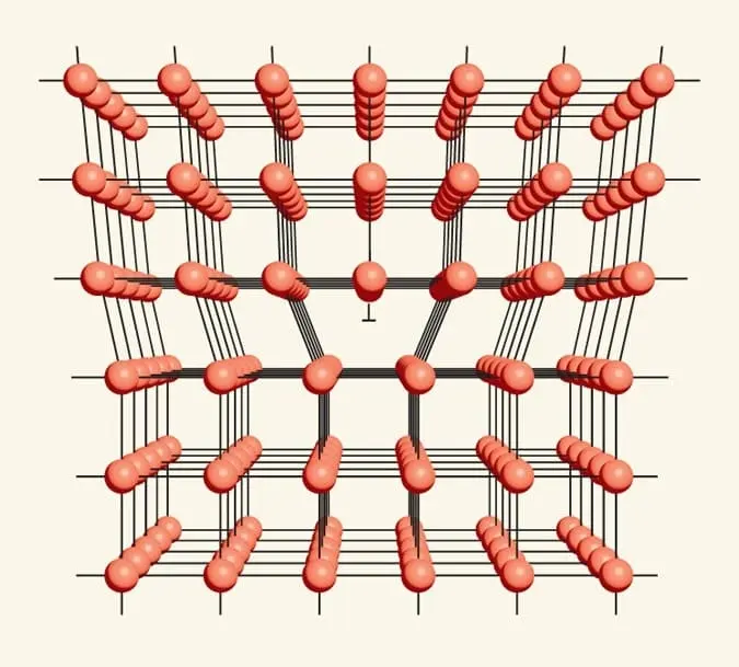
Point Defects
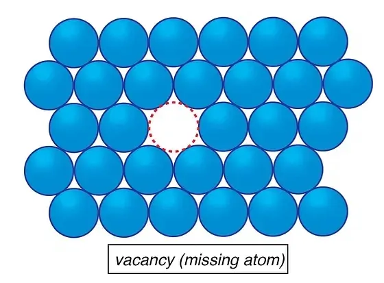
Dive deep into the atomic realm, and you’ll encounter point defects. These zero-dimensional defects are subtle yet impactful. They appear as either vacancies, where atoms are missing from their rightful places, or interstitials, where rogue atoms sit in positions they ideally shouldn’t.
Line Defects
Visualize lines or strings running through the crystal lattice, and you’re picturing line defects. Prominent among these are dislocations. Depending on their nature, they might slide, twist, or remain unmoved. Their behavior significantly determines how easily a material can be bent, molded, or reshaped, impacting its overall mechanical attributes.
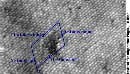
Surface Defects
On the outer facade of crystals, one can encounter surface defects. These two-dimensional defects aren’t just superficial. Grain boundaries, twin boundaries, and more play crucial roles, especially during processes like annealing, where grains grow and determine the material’s macroscopic properties.
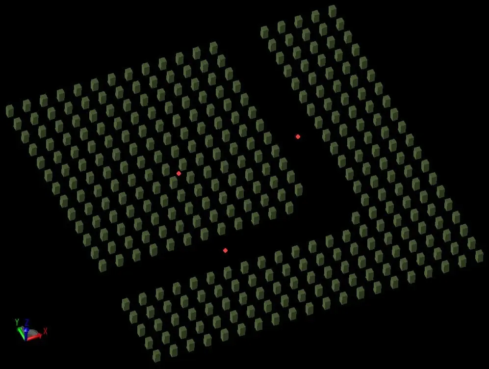
Volume or Bulk Defects
Diving into the very heart of the crystal structure, one finds volume defects. Occupying three-dimensional spaces, they manifest as pores, voids, or even cracks.
Additionally, inclusions, which are foreign materials or particles, might be trapped, influencing the crystal’s overall strength, transparency, and other properties. The presence of these defects can greatly impact the material’s durability and resistance to external forces.
Root Causes of Crystal Defects
The intricate world of crystals is often marred by defects, some occurring spontaneously, while others are consequences of external influences. Although these defects can sometimes be seen as natural imperfections or anomalies, they can also be initiated, intensified, or prevented based on certain conditions.
Inherent Imperfections
During the process of crystal growth, conditions are not always pristine. Factors like the purity of the initial materials, the equipment used, and even the surrounding environment can play a significant role. Rapid cooling can cause the crystal lattice to form haphazardly, leading to imperfections. Similarly, if there are competing growth directions, it can cause the crystal lattice to misalign, introducing more defects. These are intrinsic imperfections that arise due to the very nature of the crystal formation process.
Thermal Dynamics
Temperature is a pivotal factor in determining the structure and quality of crystals. Elevated temperatures can be a double-edged sword. On one hand, they provide the energy required for crystal formation, but on the other, they can induce chaos at the atomic level. When exposed to high heat, atoms can vacate their ordained spots, creating voids known as vacancies. Others, pushed by the intense energy, might cram into places where they shouldn’t ideally be, forming interstitial defects.
External Stressors
Mechanical forces or stresses, whether it’s due to grinding, bending, or even the sheer pressure of surrounding materials, can push atoms from their ideal positions. When atoms are forcibly realigned, it can result in the formation of dislocations, which can influence a material’s malleability and strength.
Radiation Impact
The modern world relies heavily on various forms of radiation, from the benign ones used in medical imaging to the more potent types in nuclear reactors. High-energy radiation, especially X-rays or gamma rays, can disrupt the atomic tranquility of a crystal. This energetic jostling can displace atoms, leading to the creation of point defects.
The Double-Edged Sword: Effects of Crystal Defects
Defects in crystals are akin to double-edged swords; they can both enhance and undermine the properties of the material.
Enhancing Desired Properties
By intentionally introducing specific defects into crystals, scientists and engineers can tailor the material’s properties. This deliberate process, known as doping, is pivotal in the world of electronics. Semiconductors, which are the heart of most modern devices, rely on this controlled introduction of defects. By doing so, they can regulate electrical conductivity, optimizing the material for specific applications.
Detrimental Impacts
However, not all defects are welcome. Some can compromise the mechanical strength of a material, making it more prone to breaking or fracturing. Others might scatter light, reducing the material’s transparency, which is detrimental in applications like optics. Moreover, in scenarios where pure electrical conductivity is desired, defects can act as roadblocks, impeding the smooth flow of electrons.
Harnessing Defects: The Future of Material Science
The frontier of material science lies not in creating perfect, defect-free crystals, but in mastering the art of manipulating these defects. Innovations are on the horizon. Scientists are inching closer to creating superconductors that function at room temperature, which could revolutionize energy transfer. Similarly, by controlling defects, they’re crafting ultra-hard materials that could redefine construction, manufacturing, and even jewelry.
Conclusion
In the grand tapestry of materials, crystal defects stand out as both challenges and opportunities. These minute imperfections, often invisible to the naked eye, have the power to determine the destiny of a material. As our understanding deepens, the ability to recognize, classify, and harness these defects will pave the way for unprecedented innovations. The future of material science, it seems, lies not in erasing these defects but in wielding them as tools to craft the materials of tomorrow.
FAQs
- 1.Why are some crystal defects intentional?
- Deliberate defects, such as those in semiconductors, modify properties like electrical conductivity, enabling the creation of advanced electronic devices.
- 2.Can we eliminate all defects in a crystal?
- While refining techniques can reduce defects, it’s nearly impossible to create a perfect crystal without any imperfections.
- 3.How do defects influence gemstone quality?
- In gemstones, clarity is a quality parameter. Fewer visible defects mean higher clarity and value. However, some inclusions can add uniqueness and character.
- 4.Do defects affect a material’s melting point?
- Yes, defects can influence melting points. Grain boundaries, for instance, can serve as initiation points for melting.
- 5.How are defects detected in crystals?
- Advanced techniques like electron microscopy or X-ray diffraction can visualize and analyze defects at the atomic level.

Frank
Frank graduated from the University of Shanghai for Science and Technology, majoring in optics. As a technical engineer at Crylink Company, he deeply understands crystal materials and laser components.
Related Video(s) with this Article
Related Product(s) with this Article
Related Application(s) with this Article