
Introduction
In the realm of thin film deposition technologies, Ion Beam Sputtering (IBS) and Magnetron Sputtering (MS) occupy paramount positions due to their unique attributes and capabilities. Through this discourse, we aim to delve into the core principles underpinning these technologies, juxtapose their advantages and shortcomings, and explore the diverse domains they find application in.
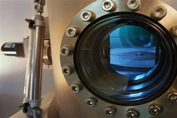
Understanding Ion Beam Sputtering: Diving into the Core Mechanisms and Characteristics
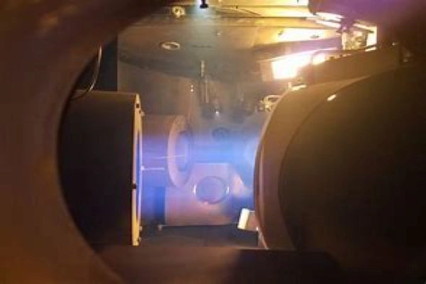
Ion Beam Sputtering (IBS) is a highly regarded methodology in the thin-film deposition landscape, instrumental in crafting high-fidelity coatings on various substrates. This technique is rooted in the precise manipulation of ionized particles, channeling them to interact with target materials, thereby initiating the process of sputtering.
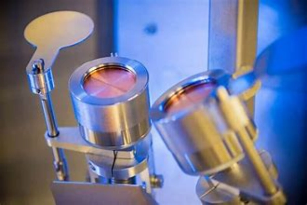
The bedrock of IBS is an ion source that generates a stream of ions. This beam of ions, under controlled parameters, is directed towards a target material. As the ions collide with the target, their kinetic energy is imparted to the atoms of the target material, leading to their ejection. These ejected atoms traverse the space between the target and the substrate, eventually settling on the substrate, and forming a thin film. The resultant film is characterized by its uniformity, compactness, and precise stoichiometric ratios, attributes that are often indispensable in high-precision applications.
A notable hallmark of Ion Beam Sputtering is its ability to yield highly uniform coatings. This uniformity is not merely superficial but extends to the atomic level, ensuring consistent properties across the film. The films are also known for their high density, which is a testament to the compact packing of atoms, minimizing voids and ensuring a robust structure. The term stoichiometric in this context refers to the preservation of the elemental composition from the target to the deposited film, which is crucial for applications where material properties are paramount.
The mastery over the deposition process in IBS is accentuated by the capability to modulate the energy and current of the ion beam. This control is pivotal as it allows for the fine-tuning of the deposition parameters, thereby enabling the customization of the coating characteristics to meet specific requirements. By adjusting the energy and current, one can influence the deposition rate, film density, and other critical attributes of the deposited film. This level of control is instrumental in achieving desired outcomes, making IBS a highly valued technique in fields where thin-film characteristics are critical to the overall performance and functionality of the end product.
Delving into Magnetron Sputtering: Uncovering the Fundamental Principles and Features
Magnetron Sputtering is a cornerstone in the realm of thin-film deposition technology, sharing the arena with techniques like Ion Beam Sputtering, yet differing in its operational principles. The fundamental ethos of Magnetron Sputtering hinges on the generation of a plasma near the target material, which is facilitated by a magnetic field.
This magnetic field plays a crucial role in confining the electrons, which, in turn, boosts the efficiency of ionization within the plasma. The heightened ionization sets the stage for a more effective sputtering process as it facilitates the ejection of atoms from the target material. As these ejected atoms travel across the chamber, they find their resting place on the substrate, gradually forming a thin film.
The narrative of Magnetron Sputtering is often highlighted by its high deposition rates. This characteristic is not merely a numerical advantage but translates into practical efficacy, especially in industrial settings where throughput is a critical metric. The higher deposition rates ensure that a substantial area can be coated in a relatively shorter span of time, thereby aligning with the demands of large-scale production environments.
Additionally, Magnetron Sputtering demonstrates a remarkable versatility in terms of the array of materials it can sputter. From metals and alloys to ceramics and compounds, the technique holds the capability to handle a broad spectrum of materials. This material versatility is not just a theoretical advantage but opens up a plethora of applications where diverse materials need to be sputtered to achieve desired functional or aesthetic outcomes.
Moreover, the scalability of Magnetron Sputtering is a feature that cannot be understated. The technology is engineered in a way that scaling up to meet industrial demands does not dilute the quality of the deposition. This scalability ensures that the transition from a laboratory setting to an industrial environment is seamless, making Magnetron Sputtering a go-to choice for a myriad of applications that span across sectors. Its adaptability to different scales of operation without compromising on the quality of the thin film makes it a robust and reliable choice in the competitive landscape of thin-film deposition technologies.
A Comparative Lens: Weighing the Merits and Demerits of IBS and MS
In the sphere of thin-film deposition, Ion Beam Sputtering (IBS) and Magnetron Sputtering (MS) are two pivotal techniques, each harboring a unique set of merits and demerits that play a critical role in determining their suitability for various applications. While their core objective of depositing thin films on substrates unifies them, the diverging operational mechanics and resulting features set them apart on a spectrum of attributes including efficiency, precision, throughput, scalability, and material versatility.
When it comes to efficiency and precision, IBS shines brightly with its inherent ability to control the ion beam. This control facilitates a highly precise and uniform deposition of coatings, rendering it an indispensable choice for applications where high precision is non-negotiable. The uniformity in coatings achieved through IBS is often of paramount importance in high-precision domains, ensuring the functional integrity of the coated products.
On the flip side, while MS is recognized for its efficiency, it may lag slightly when it comes to matching the level of precision and uniformity that IBS offers. The operational dynamics of MS, although efficient, may not provide the same level of control over the deposition process, which in turn, could lead to lesser precision in certain scenarios.
Shifting the lens towards throughput and scalability, Magnetron Sputtering takes a lead with its higher deposition rates. The capability to deposit materials at a faster pace makes MS a more favorable choice in high-throughput industrial environments. Moreover, the scalability of MS ensures that it can meet the escalating demands of industrial settings without a hitch. IBS, although robust and precise, may not align well with high-throughput requirements due to its relatively slower deposition rates, and scaling it up to meet industrial demands could pose challenges.
On the front of material versatility, both IBS and MS exhibit a commendable breadth, capable of handling a variety of materials. However, MS nudges ahead with a slight advantage due to its ability to handle an even broader spectrum of target materials. The operational principles of MS allow for the sputtering of a diverse range of materials, making it a more flexible choice in scenarios where material versatility is a crucial requirement.
In summation, the juxtaposition of IBS and MS against these critical parameters unfolds a narrative of complementary strengths and weaknesses. The choice between the two hinges on the specific demands of the application at hand, whether it’s the precision and uniformity offered by IBS, or the higher throughput, scalability, and material versatility championed by MS.
Application Horizons: Unfolding the Multitude of Domains IBS and MS are Employed In
The application horizons for Ion Beam Sputtering (IBS) and Magnetron Sputtering (MS) are indeed vast, as they cater to a multitude of domains demanding thin film deposition. These techniques embody a synergy of precision, efficiency, and versatility, making them invaluable assets across various fields.
In the optical coatings domain, IBS is often the preferred choice owing to its ability to produce highly precise and uniform coatings. The optical industry is one where the margin for error is minuscule, and the superior precision of IBS ensures the requisite optical properties are achieved with high fidelity. The uniform coatings with tight control on the stoichiometry are critical for achieving desired optical performances such as anti-reflection, high reflection, or specific spectral selectivity which is paramount in applications like lenses, mirrors, and optical filters.
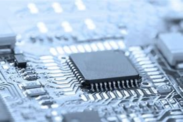
The foray of IBS and MS into the electronic and semiconductor domains underscores their versatility. In this realm, they play a pivotal role in depositing thin films on microelectronic devices, which is critical for enhancing the performance, reliability, and longevity of these devices. The semiconductor industry often demands coatings with precise thickness and material properties, and the attributes of IBS and MS are tuned to meet these exigencies, thereby aiding in the fabrication of integrated circuits, sensors, and other microelectronic components.
The aerospace and defense sectors present a challenging arena where the materials and coatings employed are expected to withstand extreme conditions. The robust coatings engendered by IBS and MS technologies are crucial in these sectors. They significantly enhance the longevity and performance of various components, providing them with the required resilience to withstand harsh environmental conditions, mechanical stresses, and corrosive atmospheres. The ability to craft durable and reliable coatings is vital in ensuring the operational efficacy and safety of aerospace and defense equipment, making IBS and MS indispensable tools in the manufacturing landscape of these critical sectors.
Thus, the application spectrum of IBS and MS is a testimony to their robustness and adaptability, making them quintessential in navigating the complex and demanding requirements of modern-day industries.
Concluding Thoughts: Gazing into the Future Trajectories of IBS and MS
As we venture forward, the continual advancements in IBS and MS technologies are anticipated to unravel new dimensions of thin film deposition, potentially fostering novel applications and improvements in existing domains. Their complementary strengths hint at a collaborative future, where hybrid techniques might surface, amalgamating the merits of both worlds.
FAQs
- What are the core differences between Ion Beam Sputtering and Magnetron Sputtering?
- The primary distinction lies in their operational principles with IBS utilizing an ion beam and MS employing a magnetic field to generate plasma for sputtering.
- Which sputtering technique is better for high-precision applications?
- IBS, owing to its controlled ion beam, is generally preferred for high-precision applications especially in optical coatings.
- Is Magnetron Sputtering suitable for industrial-scale operations?
- Yes, due to its higher deposition rates and scalability, MS is well-suited for industrial-scale operations.
- What types of materials can be sputtered using these techniques?
- A wide array of materials including metals, ceramics, and compounds can be sputtered using both IBS and MS.
- Are there hybrid sputtering techniques that combine the merits of IBS and MS?
- While there may be continual research in this domain, the emergence of hybrid techniques could potentially amalgamate the strengths of IBS and MS, paving the way for enhanced thin film deposition solutions.

Frank
Frank graduated from the University of Shanghai for Science and Technology, majoring in optics. As a technical engineer at Crylink Company, he deeply understands crystal materials and laser components.
Related Video(s) with this Article
Related Product(s) with this Article
Related Application(s) with this Article